IPC-A-610 Standard Compliance by using the Cybord Platform
Ensuring IPC-A-610 Standard Compliance by using the Cybord Platform
This guide provides an overview of IPC-A-610 Rev. G, a widely recognized standard for electronic assembly acceptance criteria. Specifically tailored for Cybord’s AI inspections, we will go into key sections of IPC, focusing on defects, corrosion, contamination, markings, and foreign object debris (FOD). By aligning our understanding with these criteria, we aim to enhance the clarity and precision of electronic component inspections. Let’s embark on a journey to ensure electronic assemblies’ highest quality and reliability.
In-depth component Analysis with Cybord
In the realm of electronic manufacturing, Cybord takes a thorough approach to inspecting components. This involves two key processes: checking the underside of components during Pick and Place (PNP) and Automated Optical Inspection (AOI) operations and examining the top side for detailed analysis.
➢Bottom Side Analysis
The pick-and-place (PnP) machine takes an image of all components right after the pick-up and before the placement to measure the alignment parameters needed for accurate placement. Cybord’s software uses this bottom-side Image to analyze the visual quality features of all mounted components. This helps identify issues like damage, corrosion, and irregularities in the structure and leads of the component. It ensures that each component meets the required standards for robustness and reliability.
➢Top Side Analysis
The AOI machine takes an Image of the assembled board from Its top side to verify that the mounting process was completed correctly. Cybord analyzes the top side images, Inspecting the markings and identifiers. This ensures that the markings are clear, accurate, match the traceability data provided, and comply with industry standards.
In the following pages, we address key requirements from the IPC standard and clarify how the Cybord platform allows compliance to be checked automatically for all assembled components.
Defects on Component leads/terminations – Section 8.2.2
The standard criteria for a defect on leads in Section 8.2.2 for Class 1, 2, and 3 is damage or deformation exceeding 10% of the lead’s diameter, width, or thickness.
Defect Assessment: Cybord meticulously examines each lead for damage or deformation exceeding 10% of the lead’s diameter, width, or thickness.
An excerpt from the standard is presented here:

Examples from images taken by the PnP machines that were disqualified by Cybord’s algorithm are presented in Figure 1.
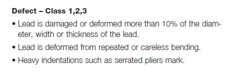
Figure 1: Examples from images taken by the pick and place machines and disqualified by Cybord’s algorithm.
Bent or warped leads – section 8.3.5.8
The standard criteria for a defect on leads In Section 8.3.5.8 for Class 1, 2, and 3 is Component lead(s) out of alignment (coplanarity) preventing the formation of an acceptable solder connection.
• Bending Evaluation: The system analyzes leads for deformation resulting from bending, ensuring compliance with IPC-A-610 guidelines.
• Indentation Recognition: Cybord’s technology is adept at detecting heavy indentations, including those caused by serrated pliers, and appropriately categorizes them.
• Coplanarity Detection: The system identifies component leads that are out of alignment (coplanarity), preventing the formation of an acceptable solder connection.
Any lead exhibiting damage beyond the specified threshold is flagged for further evaluation, contributing to fulfilling IPC-A-610 standards in electronic component inspections.
An excerpt from the standard is presented here:

Examples of bent leads and coplanarity issues appear in Figure 2.
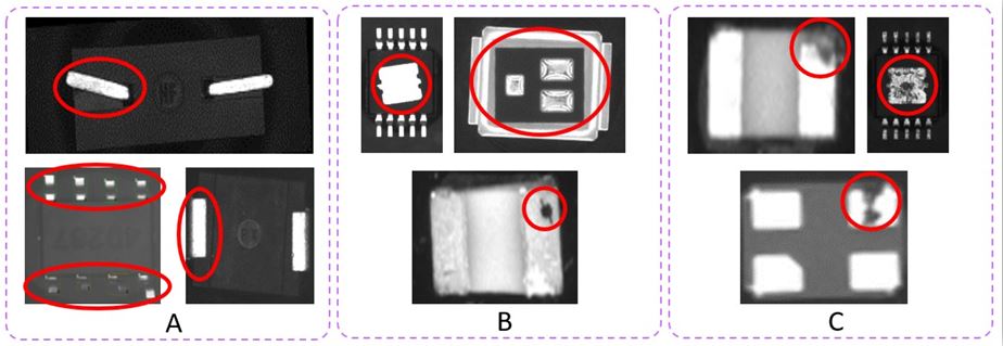
Figure 2: Examples of bent leads and coplanarity issues automatically detected by Cybord’s algorithm that exceeds 10% of the lead’s width. (A) bent leads, (B) deformed leads, (C) damaged leads.
Corrosion and Cleanliness – Section 10.6.4
In alignment with IPC-A-610 standards, Cybord is equipped to identify and evaluate corrosion on metallic surfaces or hardware, conforming to the criteria specified in Section 10.6.4 for Class 1, 2, and 3. The standard criteria for a defect – Class 1,2,3 are colored residues, rusty appearance on metallic surfaces, hardware, or evidence of corrosion. Any volume of corrosion is a defect.
• Residues Detection: Cybord’s inspection algorithm is designed to identify residues on metallic surfaces of the components, promptly recognizing any indications of discoloration.
• Corrosion Evidence Recognition: Cybord’s capabilities extend to recognizing evidence of corrosion, aligning with the defined parameters in Section 10.6.4 for cleanliness and surface appearance.
Any component or lead exhibiting residues or corrosion beyond the specified threshold is flagged for further evaluation, contributing to the fulfillment of IPC-A-610 Section 10.6.4 standard in electronic component inspections. An excerpt from the standard is presented here:

Examples of components with corrosion and contamination are presented in Figure 3.
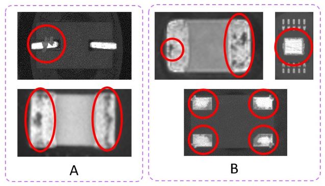
Figure 3: Examples of components with corrosion and contamination automatically detected by Cybord’s algorithm that exceed 10% of the lead’s width. (A) Contamination of leads, (B) Corrosion of leads.
Cleanliness – Foreign Object Debris (FOD) – sections 10.6.2 & 10.6.3
IPC-A-610 outlines the acceptability requirements for the cleanliness of assemblies, encompassing components with any electrical interfacing surfaces, such as connector mating surfaces and compliant pins. The standards apply to both the primary and the secondary sides of assemblies.
Contamination Evaluation: Contamination is assessed not merely on cosmetic or functional attributes but serves as a warning sign that the components containers (reels, trays) may be contaminated, mishandled, or exposed to contaminants.
The standard criteria for a defect – Class 1,2,3 in 10.6.3 is FOD not attached, entrapped, or encapsulated. Contamination, which is free to shift, and 10.6.3 refers to Cleanliness – Chlorides, Carbonates and White Residues
• Residue on the component surface.
• Residues on or around terminations.
• Metallic areas exhibiting crystalline deposits.
Any component or lead exhibiting debris beyond the specified threshold is flagged for further evaluation, contributing to fulfilling IPC-A-610 Section 10.6.2 and 10.6.3 standards in electronic component inspections.
An excerpt from the standard is presented here:


Note: The debris is typically an indicator of a root cause in the component’s handling or processing. Debris may accumulate in the mounting machine or originate from an unclean packing process at the component’s vendor, disintegrating component leads plating, etc.
Examples of components with corrosion and contamination are presented in Figure 4.
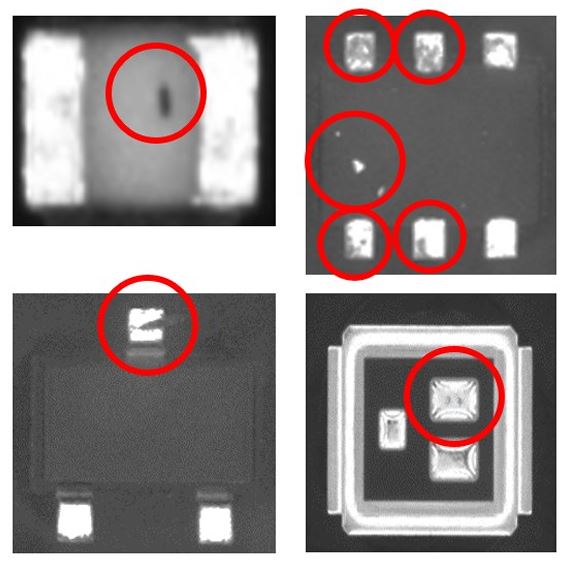
Figure 4: Examples of components with corrosion and contamination automatically detected by Cybord’s algorithm. Note that debris may be due to a component defect or point out a root cause in the supply chain, such as contaminated components in a container or poorly handled material.
Loss of Metallization – Section 9.1, 9.3
• Metallization Loss on Terminal End Face – This defect occurs when there is a discernible loss of metallization on the terminal end face, revealing the underlying ceramic material. The significance is that the ceramic’s exposure compromises the metallization’s protective layer, potentially affecting the component’s electrical functionality and structural integrity.
• Metallization Loss on Any Termination Side
In this scenario, there is a metallization loss on any side of a five-sided termination component, excluding the end face, exceeding 25% of the termination’s width or height. This defect signifies a substantial reduction in metallization coverage on a critical component surface, impacting conductivity and possibly leading to performance issues.
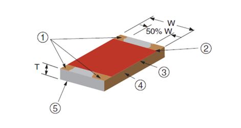
Figure 5 : Metallization loss on soldering leads.
•Irregular Shapes Beyond Specified Dimensions – Irregular shapes that deviate from the defined maximum or minimum dimensions for a specific component type.
In summary, as per IPC-A-610 standards, these metallization loss defects highlight critical vulnerabilities in electronic components, emphasizing the importance of maintaining the integrity of metalized surfaces for optimal functionality and reliability.
An excerpt from the section 9.1 of the standard for passives is presented here:

An excerpt from the section 9.3 for leaded components of the standard is presented here:

Any component or lead exhibiting metallization irregularities beyond the specified threshold is flagged for further evaluation, contributing to the fulfillment of IPC-A-610 Section 9.3 standard in electronic component inspections. Examples of components with metallization delamination is presented in Figure 6.

Figure 6 : Examples of components with metallization delamination automatically detected by Cybord’s algorithm.
Mounting Upside Down – section 8.3.2.9.2
•Defect definition – Class 1,2,3: Two-Sided Termination with Component Mounted Upside Down. When rectangular or square end chip components have one, two, three, or five side terminations, a defect is identified if the component is mounted upside down. This means that the component’s orientation is opposite to the intended configuration, which is considered non-compliant. Any upside-down component is flagged for further evaluation, contributing to fulfilling IPC-A-610 Section 8.3.2.9.2.
An excerpt from the standard is presented here:

A top-side example from the IPC standard is presented in Figure 7, and a Cybord platform’s detection of a component mounted upside down is presented in Figure 8.
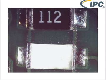
Figure 7 : A resistor mounted upside-down from the top view.

Figure 8: An example of a component mounted upside-down as automatically detected by Cybord’s algorithm. The left image is of an up-side-down component, and the right image is of a well-mounted component.
Incorrect or Missing Marking – Section 10.5
• Incorrect Marking Content: A defect is identified if the marking content is incorrect.
• Missing Marking: A defect is recorded when the marking is:
o Missing or Illegible Characters: Characters in the markings are considered defective if they are absent or not legible, jeopardizing the identification of components.
o Missing or Broken Lines Forming a Character: When lines forming a character are missing or broken to the extent that the character is not legible or is likely to be confused with another character, it is deemed a defect.
o Assembly markings, including part numbers and serial numbers, must remain legible after undergoing all tests, cleaning processes, and other procedures defined by this standard.
o Component markings and polarity indicators should be legible. Components should be mounted in a way that ensures the visibility of these markings.
• Legibility Requirements: Legibility is a critical aspect of marking standards outlined in IPC-A-610. To prevent misinterpretation or confusion during visual inspections, all characters must be clearly discernible.
Adherence to these marking standards is essential to ensure accurate component identification, compliance with electrical clearance limits, and overall legibility for successful visual inspections. Components failing to meet these marking criteria are considered defective as per IPC-A-610 standards.
All components’ top marking is analyzed for marking legibility, and the system flags any component that fails as a marking defect.
An excerpt from the standard is presented here:

The marking on all components is compared to the traceability information inputted to the production systems, and any mismatch is flagged. The mismatch represents either wrong traceability information or wrong marking information.
Examples of components with illegible markings are presented in Figure 9.

Figure 9: Examples of components with illegible markings automatically detected by Cybord’s algorithm.
Examples of wrong marking information are presented in Figure 10.

Figure 10: Examples of wrong marking information.

