Secure Hardware Assurance Using Visual AI on AOI Imaging of
Electronic Assemblies
Author: Dr. Eyal Weiss, Founder & CTO, Cybord

Abstract
Ensuring the authenticity and integrity of electronic assemblies is increasingly critical as hardware-based attacks and unauthorized component modifications become more sophisticated. Conventional inspection systems, whether rule-based AOI or traceability logs, offer limited protection against subtle or intentional tampering. This paper introduces a deep learning–based framework for secure hardware assurance that operates directly on AOI image data, enabling autonomous, full-coverage verification of every component on the board. The method is built on two previously patented systems: one for component authentication via visual fingerprinting, independent of top marking, and another for contextual decoding of top marking codes. These systems have been deployed across tens of SMT lines, generating over 5 billion productiongrade inspections. By integrating and extending these capabilities, the system performs bottom-up part analysis and top-down layout validation, identifying substitutions, rework, and tampering, without requiring electrical probing, golden boards, or metadata. Results show >99% detection accuracy and sub-second inspection times, enabling secure, imageonly verification suitable for in-line or forensic use. This work bridges the gap between software protections and physical hardware trust, transforming AOI images into a practical security and compliance enforcement tool.
1 Introduction
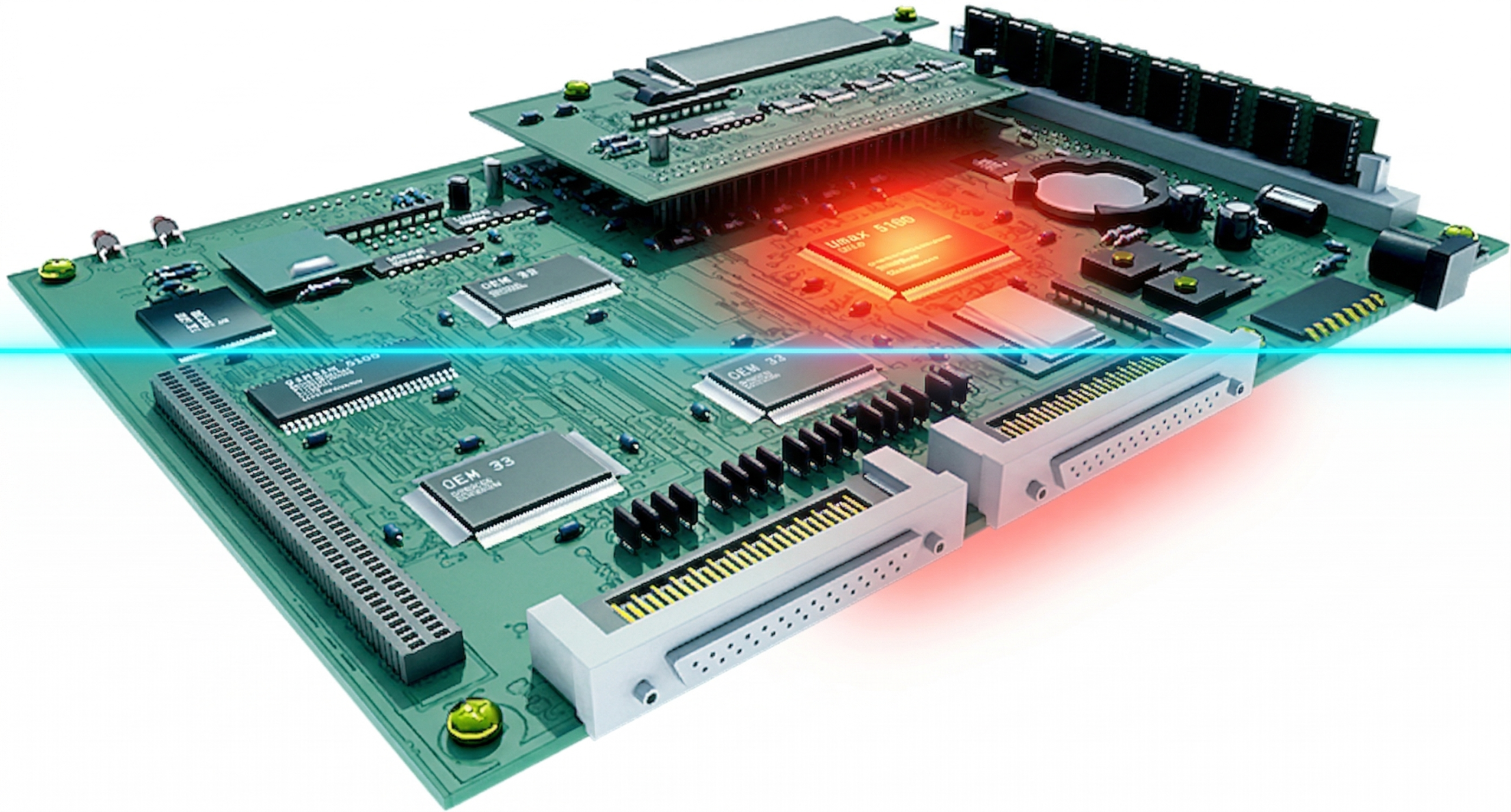
The reliability and security of modern electronic systems are increasingly challenged by component-level issues, including counterfeit parts, unauthorized modifications, and assembly inconsistencies [1–3]. These risks are particularly critical in domains such as aerospace, medical, energy infrastructure, and defense electronics, where undetected deviations can result in severe functional failures or national security breaches [4, 5]. Although Automated Optical Inspection (AOI) systems are widely used in electronics manufacturing, their scope remains limited to rule-based validation of basic attributes, component presence, orientation, polarity, leaving more subtle or undocumented modifications undetected [6–13].
Meanwhile, high-resolution AOI images, captured routinely during production, contain rich visual informationthat could reveal anomalies in shape, markings, package geometry, lead configuration, and solder interfaces. These features are rarely interpreted beyond pass/fail rules and are completely disconnected from security assurance or supply chain verification efforts [6, 10]. This limitation has come into focus in recent years. A May 2025 investigative report by Reuters revealed the presence of rogue wireless modules embedded in Chinesemanufactured solar inverters deployed across U.S. infrastructure [14]. These undocumented components were invisible to conventional inspection and enabled covert remote access that bypassed all software protections. A similar case, the widely discussed “Big Hack”, involved allegations of tiny unauthorized devices implanted onto server boards to facilitate cyber-espionage [1]. Such incidents underscore the growing disconnect between digital cybersecurity protections and the physical verification of hardware.
This limitation has come into focus in recent years. A May 2025 investigative report by Reuters revealed the presence of rogue wireless modules embedded in Chinese-manufactured solar inverters deployed across U.S. infrastructure [14]. These undocumented components were invisible to conventional inspection and enabled covert remote access that bypassed all software protections. A similar case, the widely discussed “Big Hack”, involved allegations of tiny unauthorized devices implanted onto server boards to facilitate cyber-espionage [1]. Such incidents underscore the growing disconnect between digital cybersecurity protections and the physical verification of hardware.
Current approaches to [4, 15, 16] trust rely heavily on documentation, sample testing, and presumed supplier integrity, rather than verifying the actual physical materials present on the board [3]. This results in a security blind spot: if a component is visually wrong, but electrically equivalent, or placed in an uninspected area, it is likely to go undetected. Rule-based inspection systems and traceability frameworks were never designed to catch these scenarios.
This paper addresses that gap by introducing a practical, image-based method to perform component-level [17] using the same AOI data already generated during production. Our approach enables scalable, non-invasive detection of unauthorized component [2, 16, 18–21] changes and structural anomalies, providing a critical layer of trust at the physical level, without requiring [18], golden boards, or complete traceability metadata [22–24].
This work builds on two foundational capabilities previously developed and patented by our team. The first involves visual AI–based authentication of electronic components using their physical fingerprint, geometry, lead structure, and surface finish, to identify the manufacturer regardless of top markings [25, 26]. The second enables contextual decoding of top marking codes to extract part numbers, lot/date codes, and traceability metadata. These methods have been field-proven through deployment on tens of SMT production lines, accumulating over 5 billion component inspections [27]. The current framework integrates and extends these capabilities toward full-board secure hardware assurance.
2 Method
The proposed inspection framework is designed to analyze high-resolution images generated by Automated Optical Inspection (AOI) systems [10], enabling component-level verification and anomaly detection through deep learning. It integrates object detection for identifying and localizing all components on a board, semantic segmentation [28] for analyzing component geometry and solder interfaces, and a downstream anomaly classifier that evaluates deviations from expected patterns.
This architecture allows the system to detect visual anomalies that indicate tampering, substitution, or undocumented rework, with no reliance on electrical measurements, rule-based tolerances, or golden board comparisons. The workflow, outlined in Fig. 1, includes dataset acquisition, model training, and real-time inspection on new boards.
The framework operates along two parallel tracks:
 A bottom-up component analysis, where each part is visually fingerprinted based on body shape, leads or balls, logo, top marking, and package features [25, 26];
- A top-down layout inspection, where the entire board is evaluated for missing, added, or misplaced components relative to learned spatial patterns.
This dual-layer strategy enables the system to detect both local and global deviations with high sensitivity and flexibility across board types.
2.1 Dataset and Training
Training data was acquired from two sources:
- Clean production boards, imaged inline during assembly with consistent lighting and camera setup.
- Degraded boards, collected from scrap lots and recycling centers, imaged in both cleaned and uncleaned conditions to capture real-world noise: corrosion, oxidation, broken components, dirt, and surface wear.
The use of multi-domain data ensures generalization across typical production variability and post-deployment board conditions.
The dataset was expanded using a bootstrapped training strategy [29]:
Initial models trained on pristine images were used to infer component locations and masks on degraded boards. These predictions were manually reviewed and corrected to generate new labeled examples. The updated data was used to retrain the models. This cycle was repeated until detection and segmentation stabilized across pristine and degraded conditions.
To ensure label correctness without a golden sample or external documentation, each degraded board was captured under three imaging conditions: (1) as received (degraded), (2) after air-jet cleaning, and (3) after thorough water cleaning and drying. Because these captures represent the same physical board, component identities and positions remained constant across all three images. Manual annotation was therefore performed only once, on the final, fully cleaned image where all components were clearly visible, and the resulting bounding boxes and segmentation masks were automatically registered to the other two versions through spatial alignment. This ensured accurate labels for both clean and degraded conditions while exposing the models to realistic surface noise and corrosion patterns. Visual verification of registration was carried out on a random subset of boards to confirm pixel-level correspondence between the three image conditions.
This procedure eliminated the need for golden boards or exhaustive pre-labeling and enabled the model to learn robustness to contamination, occlusion, and structural damage that typically degrade rule-based inspection systems.
The dataset and model training strategy build on two prior systems developed by our group: (1) a bottom-view authentication engine used to identify component source based on physical characteristics, and (2) a top-view marking decoder trained to read and interpret manufacturer-specific markings. Both systems have been deployed at scale in production and provided the initial models and annotation tools used in this work.
This multi-domain dataset supports model generalization across pristine, degraded, and field-recovered board conditions, critical for real-world deployment where production variability and contamination are common.
The complete dataset comprised 112 labeled boards representing multiple PCB designs and capture conditions, totaling 82,634 annotated components. Each board contained on average 737.8±836 components (median = 456, maximum = 4,894). Of these, 25 boards originated from in-line AOI machines and represent pristine production conditions. The remaining 87 boards were manually scanned and captured under three different surface conditions: (1) as received (degraded), (2) after air-jet cleaning, and (3) after thorough water cleaning and drying. Thus, each of these boards contributed three visually distinct but geometrically aligned versions, yielding realistic diversity in contamination and illumination.
All models used data drawn from this same corpus with non-overlapping splits by board design (70/20/10% for train/validation/test). This ensured that no design appeared in more than one split, providing a true measure of generalization across unseen boards.
2.2 Object Detection
Component-level object detection is performed using the YOLOv12 architecture [28, 30]. This model was chosen for its strong performance in dense scenes and its speed, enabling inference under 1000 ms per board. The detector is trained to localize and classify components by package type using CAD-aligned bounding boxes. Data augmentation techniques, flipping, brightness shifts, mild rotation, and Gaussian blur, were applied to improve generalization across lighting and contamination conditions.
In deployment, the model outputs bounding boxes, class labels, and confidence scores for each component. These detections are used both for component fingerprinting and for guiding segmentation and anomaly classification as seen in Fig. 2.
2.3 Component Segmentation
The segmentation module was designed to extract the functional sub-regions of each component, its body, leads, and pads, rather than to produce full pixel-accurate masks. Accordingly, the model operates as a semantic–instance hybrid: a U-Net–like encoder–decoder network (ResNet-34 backbone) first generates dense probability maps, which are then post-processed into geometric regions by connected-component analysis and rectangular fitting. Each resulting region corresponds to a discrete object (e.g., a pad pair or lead cluster) represented by its own bounding box and class label.
Because the final output represents object instances derived from segmentation, we evaluate performance using detection-style metrics (precision, recall, mAP50) that directly measure the accuracy of region localization. Pixel-wise IoU or Dice metrics would not fully capture the intended goal, since small boundary variations have minimal effect on geometric reasoning or downstream anomaly classification.
Training used a combined Dice + binary-cross-entropy loss to stabilize region formation, with standard augmentations (flip, rotation, brightness, and mild blur) to increase robustness. The final model consistently detected component bodies, leads, and solder interfaces even under contamination or corrosion, enabling reliable geometric feature extraction for anomaly analysis as seen in Fig. 3.
Output from the semantic segmentation model showing detailed masking of each component’s body (shown in blue) and the associated solder pad regions (highlighted in red). These masks enable fine-grained geometric comparisons with the golden reference.

2.4 Anomaly Classification
The anomaly-classification module receives features extracted from both the detection and segmentation stages and assigns each component to one of several anomaly categories. Each detected component is represented by a feature vector that combines geometric, visual, and contextual attributes:
- Bounding-box dimensions and aspect ratio.
- Pad-to-body alignment and relative spacing.
- Texture descriptors and marking-alignment cues from the component crop.
- Neighborhood relations and local density metrics within the board layout.
These geometric and visual attributes are combined through a fused encoding process.
Each cropped component image is passed through a compact convolutional encoder to obtain a visual embedding, which is concatenated with normalized geometric descriptors such as bounding-box dimensions, pad offsets, and neighborhood spacing.
The resulting feature vector jointly represents the component’s appearance and spatial context and serves as the input to the anomaly-classification network.
The feature vector is processed by a shallow convolutional–neural network composed of three 3×3 convolution layers (each followed by batch normalization and ReLU) and a fully connected layer with softmax activation over K = 7 classes: missing, added, rotated, piggybacked, contaminated, unknown, and reworked. Training used a categorical cross-entropy loss with class-balancing weights and standard augmentation on cropped component images (flips, rotations, and illumination shifts).
The classifier was trained on [N boards] boards containing approximately [N components] labeled components derived from the detection-segmentation pipeline, split 70/20/10% for train/validation/test by board design. Performance on the held-out test set achieved a macro-average precision of [P], recall of [R], and F1 score of [F1], with most residual confusion observed between rotated and reworked classes. Examples of detected anomalies are shown in Figs. 6, 7, 8 and 9.
This classifier enables the system to automatically distinguish between diverse anomaly types while remaining independent of the detection confidence, thus providing a robust semantic description of observed deviations.

2.5 Framework Overview
The full system operates as a modular pipeline:
- High-resolution AOI images are processed by the object detector.
- Detected regions are passed to the segmentation module.
- Combined features are evaluated by the anomaly classifier.
- Output anomalies are categorized and scored for downstream action (alerting, review, traceability linking, etc.).
The system operates at production speed and requires no modification to the AOI hardware or imaging process. Once trained, it performs inspection autonomously, providing board-level results in sub-second timeframes.
2.6 Top-Down Board-Level Defect Detection
In addition to per-component analysis, the framework includes a top-down inspection stage that evaluates the full board image directly. This stage is designed to detect non-normative physical variations, such as missing or added components, rogue devices, wires, blisters, stickers, or mechanical damage, while remaining insensitive to normal imaging differences such as illumination or color tone.
For each board design, several known-good boards are captured under normal production conditions. Each image is divided into overlapping tiles. A lightweight convolutional encoder learns a per-board model of normal appearance by minimizing the intra-tile feature variance across the reference set. Robust feature normalization and photometric augmentations are applied during training so that the model becomes invariant to lighting, reflection, and camera-gain changes. The resulting distribution of tile embeddings represents the board’s normative visual baseline.
When a new board of the same design is inspected, it is tiled in the same way and each tile is passed through the trained encoder. Tiles whose feature representations fall outside the normal embedding envelope, measured by robust distance metrics (e.g., Mahalanobis or percentile-based deviation), are flagged as anomalous regions.
Adjacent anomalous tiles are merged to form board-level regions of interest that correspond to physical deviations. This process highlights only genuine structural or material changes and ignores lighting-only differences.
This board-level model enables the framework to detect wide-area or non-component defects that would be invisible to component-centric inspection, while remaining robust to optical noise. Together with the bottom-up analysis, it provides complete visual assurance of the board’s integrity.
3 Experimental Results and Case Studies
To evaluate the performance of the proposed AOI image–based inspection framework, we conducted experiments across diverse datasets representing both clean production conditions and degraded, real-world boards. The evaluation focused on component detection accuracy, segmentation quality, anomaly classification, and overall robustness under varying visual conditions.
3.1 Detection and Segmentation Performance
The object detection model, based on YOLOv12, was trained using three dataset types:
- Pristine AOI images, aligned with CAD data;
- Cleaned scrap boards, scanned under controlled lighting;
- Uncleaned scrap boards, representing worst-case conditions including oxidation, broken parts, and contamination.
Model training followed the bootstrapped strategy described in Sect. 2. Training convergence over 360 epochs is shown in Fig. 4, which illustrates loss stability and generalization across the full dataset.
Model performance on unseen boards is summarized in Table 1. The model achieved an average F1 score of 0.90 across board types, with precision and recall remaining high even on degraded inputs.
These results confirm the detector’s resilience. Although performance dips under severe degradation, precision and recall remain strong, enabling reliable component localization for downstream analysis.
We note that the training and validation loss curves in Fig. 4 are provided solely to illustrate stable convergence and the absence of overfitting within the training distribution; they are not used as evidence of generalization. Generalization was assessed independently on unseen degraded boards that were excluded from both training and validation. The lower F1 score observed on heavily degraded samples (Table 1) reflects true visual degradation, corrosion, contamination, or missing optical contrast, rather than model overfitting. In practice, these conditions obscure part boundaries and markings, reducing the information available even to human inspectors. Through the bootstrapped retraining strategy, the model’s precision on such cases improved relative to the initial baseline, demonstrating that the approach can adapt to these difficult conditions without compromising clean-board performance.

The segmentation model was evaluated on 2,371 component instances across 241 AOI images. Results are shown in Table 2. High mAP50 scores demonstrate accurate mask alignment, particularly on solder pads.
The segmentation task targets geometric localization of bodies and pads rather than dense pixel labeling. Probability maps are post-processed into rectangular regions, enabling region-level evaluation with precision, recall, and mAP50, which better reflect the intended use for geometric and alignment analysis. Figure 5 shows how segmentation precision varies with confidence thresholds, illustrating consistent performance across body and pad masks.
The resolution of the shown images corresponds to the native output of the capture system. Although magnified visualization may appear coarse, these images retain full detail required for analysis, since all computations are performed on the original captured data.


3.2 Real-World Case Studies
The framework was applied to production boards to evaluate its effectiveness in detecting undocumented deviations. These real-world examples demonstrate its ability to catch anomalies that would bypass conventional traceability and AOI systems.
- In one case, a microcontroller was flagged for inconsistent markings. Visual comparison revealed it was sourced from a different manufacturer, despite electrical equivalence. The system flagged the anomaly based on shape and logo inconsistencies.
- Another board contained a passive component logged as Panasonic, but identified visually as a Vishay part. Package geometry and finish mismatches led to its classification as a substitution.
- A separate example involved a part logged as Bourns but unrecognized by the model. The system classified it as unknown, and manual inspection confirmed it was a counterfeit or unqualified device.
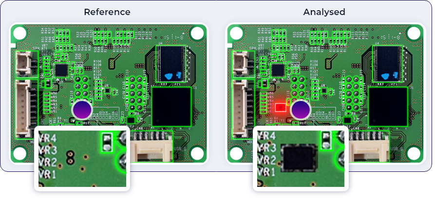
Figure 6 shows layout-level anomalies detected through top-down board inspection. Components added, missing, or misplaced relative to the learned layout are clearly flagged.
The system also detected piggybacking, a technique where unauthorized components are soldered atop legitimate ones to alter function. Figure 7 shows detection of such tampering on a board, where geometric irregularities triggered anomaly classification.
In another case, a wire had been manually soldered between two nodes post-production, likely to override circuit behavior or inject a side-channel function. Figure 8 shows this anomaly, along with an obscuring sticker, both caught by layout-based anomaly detection.
Finally, Fig. 9 shows a component substitution where a crystal oscillator was visually replaced with an alternate vendor’s part. The substitution was detected via shape, pad layout, and silkscreen misalignment.
3.3 Scalability and Throughput
Performance was benchmarked across full board scans at standard AOI resolutions. The system achieves:
- >99.3% anomaly detection accuracy.
- <0.5% false positive rate.
- <1% false negative rate.
- <1000 ms total processing time per board.
Component-level inference runs at under 10 ms per instance. This enables full-coverage inspection without disrupting throughput or requiring manual review. The framework integrates directly into post-AOI workflows and can also be applied retrospectively for forensics or supply chain audits.
4 Discussion
This work introduces a novel approach to hardware assurance: a visual AI system that performs full-coverage component-level verification using only AOI image data. Unlike conventional systems, which rely on rule-based logic, golden boards, or traceability records, our method directly analyzes the visual identity and spatial context of every component on the board, enabling the detection of anomalies that were previously undetectable at scale.
The framework described here is a direct evolution of two earlier, production-grade systems that separately addressed component-level authentication and marking interpretation. By unifying these capabilities into a board-level inspection architecture and training on a much broader dataset, we demonstrate, for the first time, scalable, component-by-component hardware assurance directly from AOI imagery.
The core novelty lies in the dual-layer inspection strategy:
- A bottom-up component fingerprinting process, where each part is analyzed individually for shape, lead configuration, markings, and logos; and.
- A top-down board-level consistency check, which learns spatial relationships across multiple known-good boards and flags layout anomalies such as missing, swapped, or added components.
Together, these layers allow the system to detect both local and global modifications, including unauthorized substitutions, rework, and tampering, without requiring any electrical testing or metadata. To our knowledge, no prior work has demonstrated this level of scalable, image-only hardware verification on production boards.
The system’s generalization ability is another key contribution. Through a bootstrapped training pipeline, it learns from both pristine and degraded board conditions, extending its performance beyond lab settings to real-world factory floors, RMA returns, or field-recovered units. This enables the method to maintain high accuracy even in the presence of oxidation, contamination, or partial damage, scenarios that defeat traditional rule-based AOI and even most learning-based defect classifiers.
Additionally, the use of standard AOI imagery makes the method immediately deployable. It introduces no production bottlenecks and requires no changes to inspection equipment. This enables manufacturers to repurpose their existing image streams, not only for quality assurance but also for supply chain verification, provenance validation, and hardware security enforcement.
While performance is strong, several practical limitations remain. The system depends on sufficient imaging quality, which can vary across AOI platforms. It also cannot determine intent, e.g., whether an anomaly stems from malicious tampering, unapproved rework, or an upstream substitution error. Expanding the component reference database and improving automated anomaly attribution will be key for scaling across product lines and sectors.
Nonetheless, this framework represents a significant evolution in how manufacturing data can be used. By combining object detection, semantic segmentation, and anomaly classification in a modular pipeline, and grounding inspection in visual pattern learning rather than rule definition, the system provides a new pathway toward trusted electronics at the physical layer.
This methodology repositions AOI imagery from a passive QA artifact to a forensic-grade security tool, enabling industries to verify not only whether components were placed, but whether the right components, from the right sources, were used.


5 Conclusion
This work presents a novel, scalable framework for secure hardware assurance based entirely on AOI image data and deep learning. By analyzing each component’s visual identity, including shape, lead structure, and markings, and comparing board-wide layouts across known-good samples, the system detects subtle anomalies such as substitutions, unauthorized additions, or tampering, without the need for electrical testing or traceability metadata.
Unlike existing inspection or authentication methods, which are limited by rules, golden boards, or metadata availability, our approach performs autonomous, full-coverage verification using data already captured in standard manufacturing workflows. This transforms AOI from a passive quality assurance step into an active layer of physical trust enforcement.
The method has been validated across a broad range of conditions, from pristine boards to visually degraded and field-returned samples, demonstrating high accuracy, generalization, and fast inference suitable for in-line deployment. Its ability to detect deviations that evade conventional AOI or software-based security makes it well-suited also for critical sectors such as aerospace, defense, and medical electronics.
By bridging the gap between image-based inspection and hardware cybersecurity, this system offers a new model for defending the physical supply chain, where hardware authenticity is no longer assumed, but verified.
This framework integrates two previously patented systems: one for identifying component origin via visual fingerprinting, and another for decoding manufacturer-specific top markings. Both have been deployed across major production lines and trained on over 5 billion AOI images. By combining these proven capabilities with board-level spatial reasoning and anomaly detection, the presented solution delivers a new standard for hardware trust at the physical layer, scalable, autonomous, and grounded in real-world manufacturing data.
Author Contributions
Eyal Weiss conceived the research, developed the methodology, conducted the experiments, prepared the figures, and wrote the manuscript. The author reviewed and approved the final version.
Data Availability
This study does not rely on publicly available datasets. All data generated or analyzed during this study are either proprietary or derived from internal operational systems and are not publicly available due to confidentiality agreements. Reasonable requests for access to anonymized data supporting the findings of this study may be considered by the corresponding author, subject to approval and compliance with relevant data protection regulations.
Declarations
Ethical Approval not applicable.
Competing interests The authors declare no competing interests.
References
1. Mehta D, Lu H, Paradis OP, Ms MA, Rahman MT, Iskander Y, Chawla P, Woodard DL, Tehranipoor M, Asadizanjani N (2020) The Big Hack explained: detection and prevention of PCB supply chain implants. ACM Journal on Emerging Technologies in Computing Systems 16:1
2. Tehranipoor MM, Guin U, Forte D (2015) Counterfeit integrated circuits. Springer, pp 15–36
3. Akter S, Khalil K, Bayoumi M (2023) IEEE Access 11:77543
4. Representatives H (2017)
5. Tehranipoor M, Pundir N, Vashistha N, Farahmandi F (2023) Hardware Security Primitives. Springer
6. Ajax R (n.d.)
7. Hemmati A, Raoufi P, Rahmani AM (2024) Edge artificial intelligence for big data: a systematic review. Neural Comput Appl 36:11461
8. Islam MMM, Emon JI, Ng KY, Asadpour A, Al Aziz MMR, Baptista ML, Kim J-M (2025) Artificial intelligence for smart manufacturing and industry X. 0. Springer, pp 9–36
9. Reshadat V, Kapteijns RAJW (2021) in 2021 International Conference on Data and Software Engineering (ICoDSE) IEEE, pp. 1–5
10. Meyer L, Josefsson B, Vrotsou K, Westin C, Lundberg J in (2021) IEEE/AIAA 40th Digital Avionics Systems Conference (DASC) (IEEE, 2021), pp. 1–8
11. Tong X, Yu Z, Tian X, Ge H, Wang X (2022) Front Comput Sci 16:1
12. Ni Y-S, Chen W-L, Liu Y, Wu M-H, Guo J-I (2024) Sensors 24:5737
13. Chen I-C, Hwang R-C, Huang H-C (2023) Processes 11:775
14. Mcfarlane S (2025) Reuters
15. Spieske A, Birkel H (2021) Improving supply chain resilience through industry 4.0: a systematic literature review under the impressions of the COVID-19 pandemic. Comput Ind Eng 158:107452
16. Gayialis SP, Kechagias EP, Papadopoulos GA, Masouras D (2022) Sustain (Switzerland) 14(11):6666
17. Rahman MT, Shi Q, Tajik S, Shen H, Woodard DL, Tehranipoor M, Asadizanjani N in (2018) IEEE 3rd International Verification and Security Workshop (IVSW) (2018), pp. 93–102
18. Tehranipoor MM, Guin U, Forte D (2015) Counterfeit integrated circuits. Springer, pp 95–107
19. Tehranipoor MM, Guin U, Forte D (2015) Counterfeit integrated circuits. Springer, pp 75–93
20. Kessler LW, Sharpe T (2010) Print Circuit Des Fab 27:64
21. a S, Report (2011) T
22. Razak GM, Hendry LC, Stevenson M (2023) Supply chain traceability: a review of the benefits and its relationship with supply chain resilience. Prod Plan Control 34:1114
23. Rosales P (2021)
24. Schuitemaker R, Xu X (2020) In Procedia CIRP, vol. 93. Elsevier B V, pp 700–705
25. Weiss E (2024) Electronic components provenance assurance through AI and big data in assembly processes. IEEE Trans Compon Packag Manuf Technol 14(11):2107–2115
26. Weiss E (2021) SMTA
27. Weiss E, Efrat Z (2021) P-603538-PC
28. Li Y, Duan Y, Duan L, Xiang W, Wu Q (2024) in Medical Image Understanding and Analysis, edited by M. H. Yap, C. Kendrick, A. Behera, T. Cootes, and R. Zwiggelaar Springer Nature Switzerland, Cham, pp. 143–159
29. Grill J-B, Strub F, Altché F, Tallec C, Richemond PH, Buchatskaya E, Doersch C, Avila Pires B, Daniel Guo Z, Gheshlaghi Azar M, Piot B, Kavukcuoglu K, Munos R, Valko M (n.d.) Bootstrap Your Own Latent A New Approach to Self-Supervised Learning
30. Li Y, Li S, Du H, Chen L, Zhang D, Li Y (2020) IEEE Access 8:227288
Publisher’s Note
Springer Nature remains neutral with regard to jurisdictional claims in published maps and institutional affiliations.
Springer Nature or its licensor (e.g. a society or other partner) holds exclusive rights to this article under a publishing agreement with the author(s) or other rightsholder(s); author self-archiving of the accepted manuscript version of this article is solely governed by the terms of such publishing agreement and applicable law.