The European Union is preparing its next major semiconductor push. SEMI Europe recently released comprehensive recommendations for a CHIPS Act 2.0, calling for deeper investment across the full semiconductor value chain, from R&D and chip design through materials, equipment, and both front- and back-end manufacturing. The stated goal is ambitious: reduce Europe’s strategic dependency and build genuine end-to-end capability on the continent.
By: Oshri Cohen, CEO, Cybord AI
The stakes are real. Europe currently produces less than 10% of global semiconductors while consuming roughly 20% of worldwide chip output. Closing that gap requires sustained, coordinated investment, and the SEMI Europe recommendations provide a serious blueprint for doing so.
But there is a structural reality embedded in the current CHIPS Act framework that CHIPS Act 2.0 has not yet fully resolved, and that manufacturers and OEMs operating in Europe should pay close attention to.
Where the funding has actually gone
The original CHIPS Act directed most of its Pillar II investment toward front-end fabs: wafer fabrication, silicon processing, the high-profile plants that make headlines. This was not accidental, fab investment is visible, capital-intensive, and directly tied to Europe’s stated 20% global market share target.
Back-end manufacturing, the outsourced semiconductor assembly and test (OSAT) phase where chips are packaged, tested, and prepared for integration into finished electronics, received far less strategic attention. The SEMI Europe position paper for CHIPS Act 2.0 acknowledges this explicitly, recommending that the FOAK (First-of-a-Kind) definition be expanded to include the full value chain, and that new facility categories be created to cover chip design, materials, components, and equipment beyond the existing Integrated Production Facility and Open EU Foundry labels.
This is an important correction. But it raises a practical question for the electronics manufacturers: who will ultimately assemble these components into finished systems. Even if European fab capacity grows substantially, where will final assembly happen?
The offshore assembly reality
For most product categories – consumer electronics, industrial controls, telecom equipment, server hardware – final assembly will continue to occur in Asia for the foreseeable future. OSAT capacity in Taiwan, South Korea, Malaysia, and China is deeply entrenched, highly specialized, and not something that policy investment alone can relocate in a five-year window.
This is not a failure of CHIPS Act 2.0. It is a realistic assessment of how global electronics manufacturing is structured. What it means, however, is that European policy ambition and actual manufacturing reality will diverge at the assembly stage for years to come.
This creates an implicit risk vector that the policy debate has not adequately addressed: components verified and traced through European fabs and supply chains will, in many cases, converge with components from other sources at offshore assembly lines, where European oversight ends.
The SEMI Europe paper correctly identifies that “resource supply and demand of advanced semiconductor technologies” must align, and that “supply chain security and resilience” must be central to the strategy. But supply chain security is not only a fab-level problem. It is an assembly-level problem too.
What the policy shift implies for manufacturers
The trajectory of CHIPS Act 2.0, with its emphasis on traceability, trusted supply chains, and end-to-end European capability, creates a new compliance and expectations environment, even for manufacturers whose assembly operations remain offshore.
If European policy increasingly demands provenance verification and component-level traceability as conditions of market access or funding eligibility, the expectation will not stop at the fab gate. It will extend to the assembly line, wherever that line happens to be located.
In practical terms, this means that OEMs and electronics manufacturers will face growing pressure to demonstrate what actually happens at the point where components are placed on boards. Supplier declarations and batch-level documentation, already insufficient under standards like IPC-1782B and the US CHIPS Act’s country-of-origin requirements, will come under further scrutiny as the European regulatory environment matures.
The SEMI Europe paper notes that Europe currently faces a supply chain where “lack of market demand and semiconductor talent gap are the primary concerns of semiconductor companies investing in Europe.” Demand-side confidence, in turn, depends on trust in the hardware stack. And hardware trust cannot be asserted through paperwork alone, it requires verified ground truth at the component level.
The verification gap at final assembly
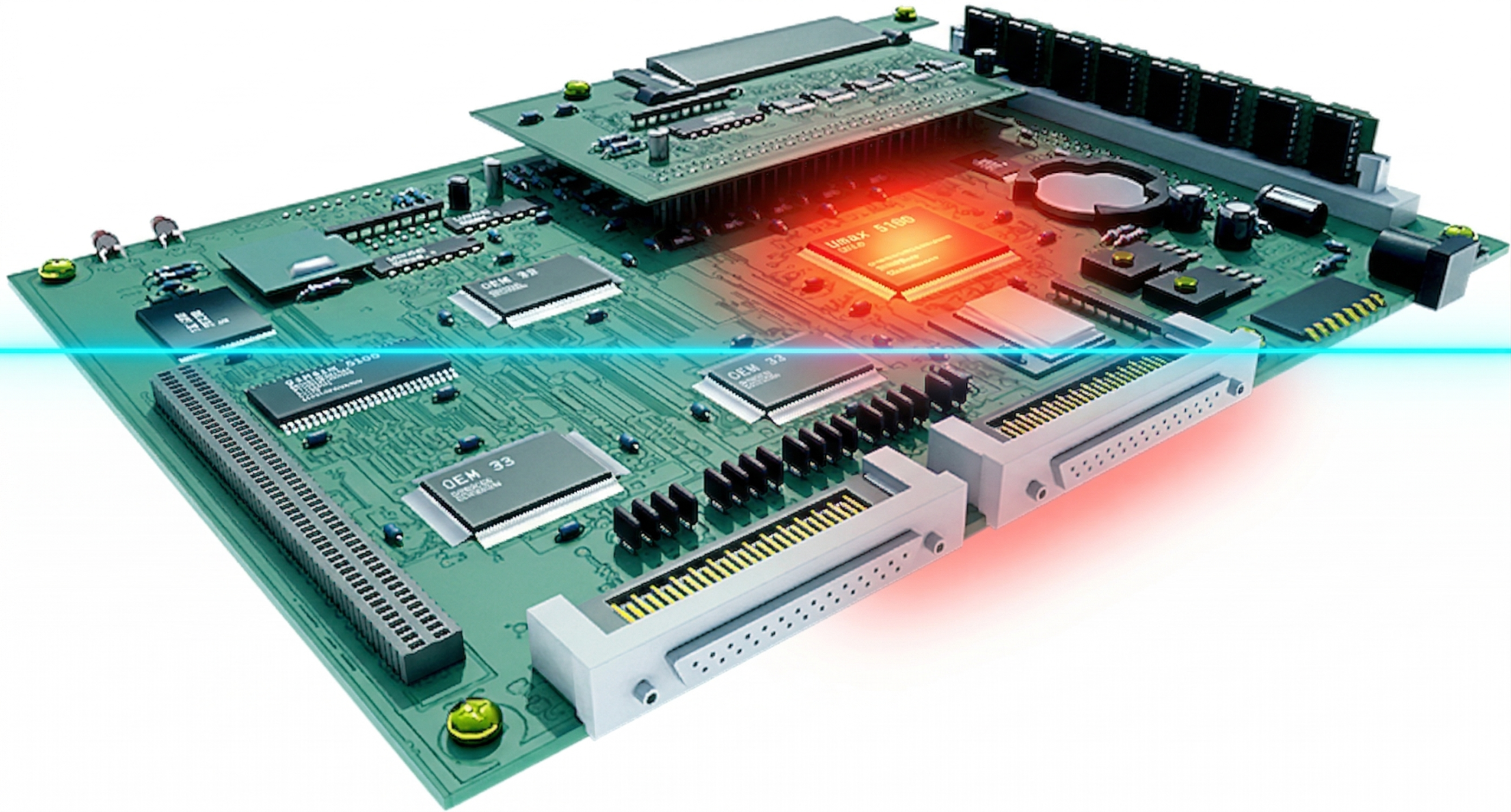
Consider what happens on a typical SMT production line. A server board may contain 2,000 or more individual components. Those components arrive from multiple suppliers across multiple geographies, with varying documentation quality and supply chain histories. Traditional incoming inspection methods, sampling-based, documentation-dependent, were not designed for the level of assurance that critical infrastructure now requires.
A data center operator deploying AI infrastructure in Europe, an automotive OEM certifying safety-critical systems, a telecom equipment provider supplying 5G base stations across European networks – all of them face the same underlying exposure: the inability to confirm, at the individual component level, what was actually installed in their products.
This is not a hypothetical concern. Industry bodies including ERAI, SAE International, and the US Department of Defense have documented repeated instances where counterfeit or unauthorized components bypassed traditional quality checks and were only identified after field failures or teardown analysis.
The question CHIPS Act 2.0 must prompt manufacturers to ask is straightforward: if European policy is moving toward verified, trusted, end-to-end supply chains, how do you demonstrate compliance at the one point in the process where your components become your product?
Transparency at assembly is now a strategic requirement
Several verification approaches can address this gap. Automated optical inspection integrated directly into SMT production lines can analyze components at placement speed, comparing visual characteristics against manufacturer specifications and detecting signs of substitution, counterfeiting, or tampering. Advanced inline verification systems can capture and decode top markings, manufacturer identifiers, lot codes, date codes, country-of-origin markings, generating a verified record of every component placed on every board.
The key requirement is that these approaches operate in-line, at production speed, without adding handling steps or slowing throughput. Manufacturers will not adopt verification methods that impose operational costs disproportionate to their compliance benefit.
Beyond any specific technology, what matters is the principle: assembly-line transparency must become a deliberate capability, not an afterthought. The Zero Trust principle that has reshaped cybersecurity, trust nothing, verify everything, applies with equal force to hardware manufacturing. Assuming that components arriving at an assembly line are authentic and compliant is a policy liability, not just an operational one.
The SEMI Europe recommendations are right to push for end-to-end European capability, simplified access to state support, and stronger industry-policy consultation. But end-to-end capability means end-to-end verification. A chip that is designed in Europe, fabricated in a trusted European facility, and then assembled in an offshore process that cannot be audited at the component level is not a verified product; it is a partially verified product.
What manufacturers should be doing right now
CHIPS Act 2.0 is in its recommendation phase. Regulatory expectations will evolve as the framework develops. But manufacturers who wait for final regulations before addressing the assembly verification gap will find themselves behind, both operationally and in terms of customer and policy confidence.
The practical steps are clear: audit your current inspection coverage at the assembly stage, identify the gap between what your documentation claims and what you can actually verify, and evaluate whether your current inspection infrastructure can generate the component-level traceability that emerging standards and policy expectations will require.
Europe’s semiconductor ambitions are serious and well-funded. The manufacturers and OEMs who will benefit most from that investment are the ones who recognize that supply chain resilience does not end at the wafer fab, it ends at the last component placed on the last board of every finished product.
View the Related Posts section below to learn more about component-level verification and manufacturing transparency at cybord.ai.
About the author:
Oshri Cohen is the CEO of Cybord. He brings over 20 years of leadership experience in global supply chain and operations, including 15 years in senior roles at NVIDIA and Mellanox Technologies, where he led complex manufacturing and supply chain organizations at scale.
References
SEMI Europe – Policy Recommendations for a Chips Act 2.0 (April 2026)